discover the world beyond your sight

Test | Measurement Solutions

The Opto Imaging Modules are available with integrated, diffuse LED ring light illumination in fixed and segmented versions and a coaxial incident LED. Many magnifications, working distances and optical contrast techniques are available within the different form factors. USB 3.0 versions or GigE versions for machine builders and integrators.

Applications

  • SMD Inspection
  • Image-Based Hardness Testing
  • Crimp Analysis
  • Quality & Control Needs
  • Documentation Units
  • Industry 4.0 Sensor Solutions
  • Overview & Detail Digital Zoom

Solutions For Optical Quality Control

Test & Measurement refers to all industrial applications in which microscopic structures have to be displayed and analysed. 

Here are some examples where the imaging modules are used:

  • Semiconductor technology, SMD inspection, solder joint analysis
  • Automotive, quality control, process control, cylinder inspection
  • Metallography (hardness testing, crimp analysis, weld seam control) 
  • Energy, solar wafer inspection

Fabrics, Filter and Sieves Measurement and Classification

Optical measurement of mesh widths with the compact ‘Profile Projector’

In contrast to mechanical test methods using test sand or glass balls, optical measurement of the mesh dimensions is a fast and reliable measurement method and ideal for inline control of production results in an industry 4.0 environment.

The evaluation of the mesh size distribution and the traceability to corresponding standards such as ASTM E 11 can be realized with the new Imaging Module Profile from Opto.

The Profile Projector comes factory pre-calibrated. Opto offers calibration standards with and without DKD certificate to regularly recalibrate the optics.

The Profile Projector works with a telecentric brightfield illumination and a coordinated telecentric lens in transmitted light.

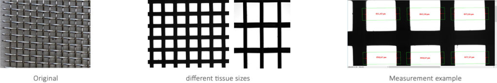
Metallurgical Sample Analysis with Opto's Machine Vision Microscopes

Customer-Task

  • Grain & Structure Analysis of Metals
  • Predictive Maintenance of production processes
  • Quality control of mechanical parts
  • Damage evaluation of metal malfunction
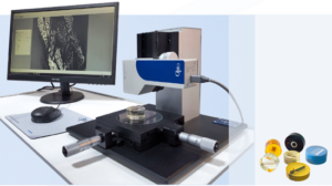
Solution

  • Imaging Module compact M (MVM) with integrated ring- and coaxial illumination
  • Small footprint with portable stand and case
  • Easy to use and free OptoViewer 2.0 software
  • Direct measurement without calibration

Advantages for the customer

  • Pure all-in-one digital microscope
  • Micrometre/pixel Resolution with large field of view
  • High Contrast and Colour stability
  • Repeatability of Image

Wafer and PCB Inspection with Imaging Modules

Tasks

  • Optical defect analysis, quality control & documentation of ICs, FPGAs, BGAs

  • One-sided, two-sided or multilayer PCB inspection

  • Detection of cracks, short circuits, defective electrical connections or bridges

  • Optical post-bond/post-reflow inspection with pin counting and component identification

  • Detection of irregularities in wafer coatings

  • Analysis of impurities, cracks or identification of particles and scratches

Solution

  • Compact M or Linea XL in monochrome or colour version
  • Application-optimized optoelectronics available in USB 3.1 or GigE – Plug & Play
  • Easy-to-use and free OptoViewer 2.0 software
  • Various Software Development and toolkits, as well as BV plug-ins for machine integration

Added value

  • All-in-one digital microscope optimized for mobile use
  • More compact than conventional microscopes 
  • Reliable image data with the highest image quality and good colour fidelity
  • Good price-performance ratio with software support

Wafer screening with a digital microscope compact M

A compact M digital microscope from the Imaging Module family is ideal for analyzing reflective wafer surfaces and displaying the smallest structures. The following features are unique to a single vision sensor:

  • Integrated coaxial brightfield illumination
  • Compact and robust design 
  • Quick change between different modules
  • Apochromatic corrected microscope optics with a long working distance
  • 5MP IMX Sony image sensor
  • Open software architecture with own Software Development Kit

Weld Inspection

The Analysis of welding results is a typical challenge of Metallography labs.

The Machine Vision Microscope with Coaxial Light and with Ring Light is perfect for Micro weld inspection.

One Plug and play Digital Microscope. No change of Equipment.

  • Magnification: 3,75x,
  • Field of View: 2,2×1,8mmWD 36mm
  • 5MP Sony IMX264 monochrome
  • – USB 3.1, 0.9 µm/Pixel
  • With the free OptoViewer, it is also possible to execute pre-calibrated measurements easily

Hardness Testing (Vickers & Brinell)

Micro Hardness Testing needs high-end optical microscopy images.
Opto has been delivering years of Imaging Modules in existing Machinery.

Solino can principally disrupt this business because:

  • with Solino, we can detect micro indents on a big surface by analyzing the reflections
  • it is possible to identify the position of a μm size indent on a big area with a standard camera
  • Solino analyses anomalies and offers reliable info about an indent of the object’s surface
  • this makes the vision set up independent of the object’s surface or ambient light conditions
Scroll to Top